


Most people like
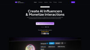
MakeInfluencer AI

 90.8K
90.8K
 50.53%
 4
4
Create and monetize AI influencers for audience engagement.
AI Character
AI Social Media Assistant
AI Bio Generator
AI Content Generator
AI Avatar Generator
AI Profile Picture Generator
AI Chatbot
AI Instagram Assistant
AI Twitter Assistant
AI Facebook Assistant
AI Tiktok Assistant
AD
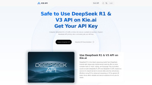
Kie.ai: Affordable & Secure DeepSeek R1 API
< 5K
1
Affordable DeepSeek R1 API with powerful reasoning and robust security.
AI Productivity Tools
AD
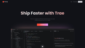
Trae
1M
 44.54%
1
44.54%
1
Adaptive AI IDE that helps you ship faster.
AI Code Generator
AD
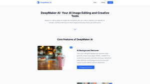
DeepMaker AI
< 5K
4
AI Image Editing Tools for Professionals
Text to Image
Photo & Image Editor
AI Tattoo Generator
AI Manga & Comic
AI Background Remover
AI Profile Picture Generator
AI Photo Restoration
AI Photo Enhancer
AI Logo Generator
AI Photo & Image Generator
AI Image Enhancer
AI Icon Generator
AI GIF Generator
AI Emoji Generator
AI Background Generator
AI Avatar Generator
AI Illustration Generator
AI Face Swap Generator
AD
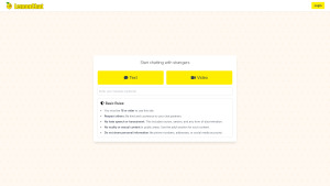
LemonChat
76.7K
 50.9%
1
50.9%
1
Chat anonymously with strangers via text or video.
AI Chatbot
AD
Are you spending too much time looking for ai tools?
- App rating
- 4.9
- AI Tools
- 100k+
- Trusted Users
- 5000+
 WHY YOU SHOULD CHOOSE TOOLIFY
TOOLIFY is the best ai tool source.
Browse More Content
AI News CN
- ChatGPT如何进行SEO关键词研究
- GPT-4o:全新ChatGPT免费提供给所有人!OpenAI春季更新
- OpenAI发布GPT 4 Omni模型:颠覆人工智能的新里程碑
- Open AI令人难以置信的GPT-40模型!真正的游戏改变者!
- GPT 45:开创人工智能与人类对话新篇章!
- 开放AI GPT-40:AI的未来之路
- Chat GPT 4o: 声音真实到难以置信!
- 阅读和写作的重要性以及在人工智能时代的价值
- GPT发布新功能!iPhone与GPT合作?Luisito Comunica和Jimmy的强烈指责!
- Rushchat.AI: A New Era of NSFW AI Companionship
Related Articles


Refresh Articles
